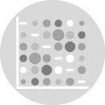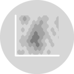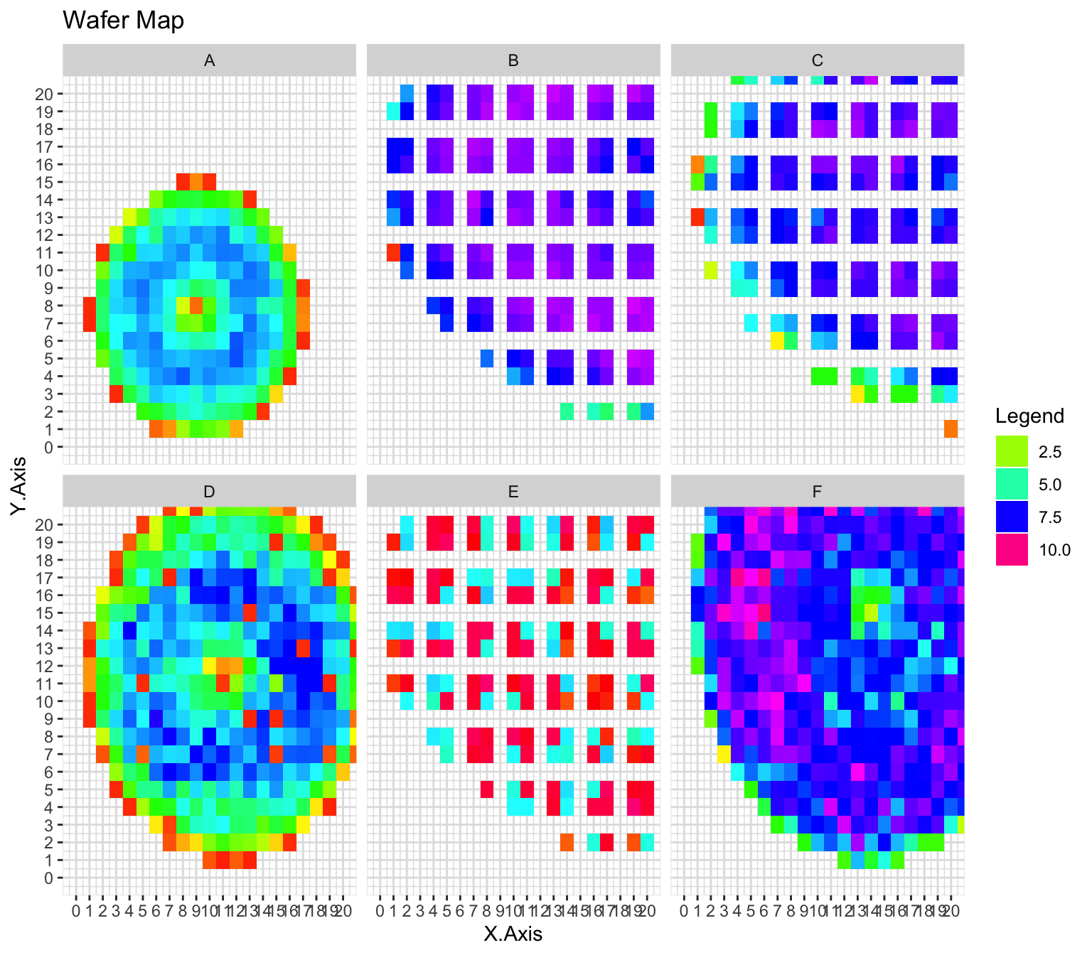
A wafer map is used to visualize the performance of a semiconductor device on a substrate. Each rectangle represents an individual semiconductor chip and its colour or pattern can represent some property of the chip.
Data used as input in this examples are available here.
Thanks to to Alex Pavlides from Mango Solution for this submission!
# load data
madeUp=read.table("https://raw.githubusercontent.com/holtzy/R-graph-gallery/master/DATA/madeUp.csv", sep=",", header=T)

# load libraries
library(tidyverse)

# Prepare data
theData <- madeUp %>%
 group_by(X.Axis, Y.Axis, Group) %>%
 dplyr::summarize(statistic=mean(randVals, na.rm = TRUE))

# plot
ggplot(theData, aes(X.Axis, Y.Axis)) +

    coord_cartesian(xlim = c(0,20), ylim = c(0,20)) +
    scale_x_continuous(breaks = seq(0,20)) +
    scale_y_continuous(breaks = seq(0,20))+

    geom_tile(aes(fill=statistic))+
    guides(fill=guide_legend(title='Legend'))+

    theme(
        panel.background = element_rect(fill= 'white', color = 'white'),
        panel.grid.major = element_line(color='#E0E0E0'),
        panel.grid.minor = element_line(color='#E0E0E0')
        )+

    ggtitle('Wafer Map')+
    facet_wrap(~Group)+
    scale_fill_gradientn(colors = rainbow(100))